Atomic Layer Deposition
-
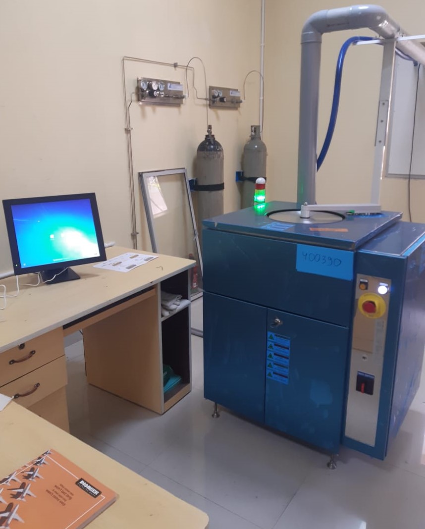
Name of the equipment/facility: Atomic Layer Deposition
-
Model: PICOSUNTM R-200
-
Working Principle : Atomic layer deposition (ALD) is a thin-film deposition technique based on the sequential use of a gas-phase chemical process; it is a subclass of chemical vapour deposition. The majority of ALD reactions use two chemicals called precursors (also called ). These precursors react with the surface of a material one at a time in a sequential, self-limiting, manner. A thin film is slowly deposited through repeated exposure to separate precursors. ALD is a key process in fabricating semiconductor devices, and part of the set of tools for synthesising nanomaterials.
Technical specification & Applications:
KEY Features:
- Capability to deposit dielectric oxides such as Al2O3, ZnO, HfO2, TiO2 .
- The following materials can be deposited at < 100o C: Al2O3, ZnO, HfO2, TiO2.
- Tools operate from RT to 500o C with heater elements located in the intermediate space between the reaction chamber and vacuum chamber walls.
- Air cooled ALD reactor
- ALD tool can accommodate wafers up to 200 mm diameter and small-medium sized 3D objects (max height ca. 130 mm).
- Non-uniformity values of the following oxides are < ± 1 %. Some RECORD non-uniformity values as an example:Al2O3: 0.13%, ZnO:0.94%, TiO2:0.28%
- Tool can handle liquid, solid and gas precursors.
- The tool has 4 fully separated precursor lines and inlets.
- cycle time ≤ 2 s can be achieved
- It is suitable heating up to 300oC.
Applications:
- Semiconductor Engineering
- Li-ion Batteries
- Microelectromechanical systems (MEMS)
- Conformal and nano-coatings
- Fuel cells
- Solar cells
- Transistors
- Drug Delivery
- Tissue Engineering
- Implant


